
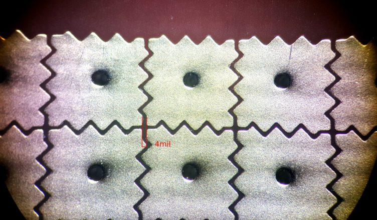
Following the simulations of electrodes a smaller gap between the electrodes and a more important overlap should improve the performance of the device. The first OpenDrop devices have been produced on a standard printed circuit board (PCB) manufacturing process with smallest features (gaps & traces) of 8 mil (0.2 mm). The still quite standard fine process of PCB manufacturing allows for feature sizes down to 4mil (0.1mm). The new electrode design takes advantage of this and the gaps are reduced to 4mil.
In the process of producing the new design the PCB manufacturer (PCBWay.com) choose the wrong process and enlarged the gap between the electrodes to 8mil again. Communication with the manufacturer in Shenzhen was however very constructive and the OpenDrop V2.1 design was remade by the factory using the correct 4mil process. The reason for the error may be that it was not clear to the manufacturer to use 4mil process as only the electrode gaps were designed in 4mil and the rest of the board used standard precision. It is so recommended to point this out when ordering the boards. The good thing about the double production is that we now have identical designs with 4mil and 8mil gaps what allows us to do comparison of the two.
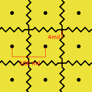
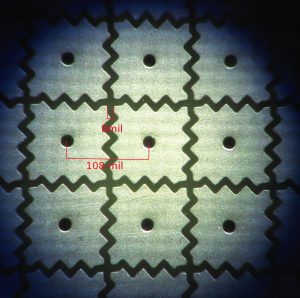
Gerber file showing electrodes in 108 mil (2.75 mm) grid with 4mil gaps in between.
Electrodes produced with 8mil process.